
Semiconductor Fixtures & Jigs Manufacturer
Production-critical tooling engineered for repeatable positioning, cleanroom compatibility, ESD control, and stable yield.
Built for Semiconductor Manufacturing Reality
Semiconductor tooling fails when it introduces uncertainty—particles, static, drift, or deformation. Our fixture philosophy is built around real fab constraints.
-
Contamination Awareness: Minimized abrasion, reduced dead corners, and serviceable contact surfaces.
-
Process Alignment: Precise control over vacuum stability, clamp force, and thermal deformation.
-
ESD Control: Explicit grounding designs with measurable contact resistance approach.
What Breaks Yield—and How We Prevent It
Engineering solutions to the four most common failure points in semiconductor handling.
Particle-Related Fluctuation
Rubbing, friction wear, and debris traps introduce contamination.
Prevention: Geometry designed to reduce rubbing, low-particle material choices.
Warpage & Locating Drift
Thin substrates slip or warp under mechanical stress.
Prevention: Datum-first locating, zoned vacuum strategy, and gentle support.
ESD Damage Risk
Static discharge during handling destroys sensitive packages.
Prevention: Design-visible grounding paths and dissipative material selection.
Unstable Contact in Test
Inconsistent mechanical alignment causes electrical test failures.
Prevention: Separating “locate” from “contact” with high-precision modular interfaces.
What We Build for Semiconductor
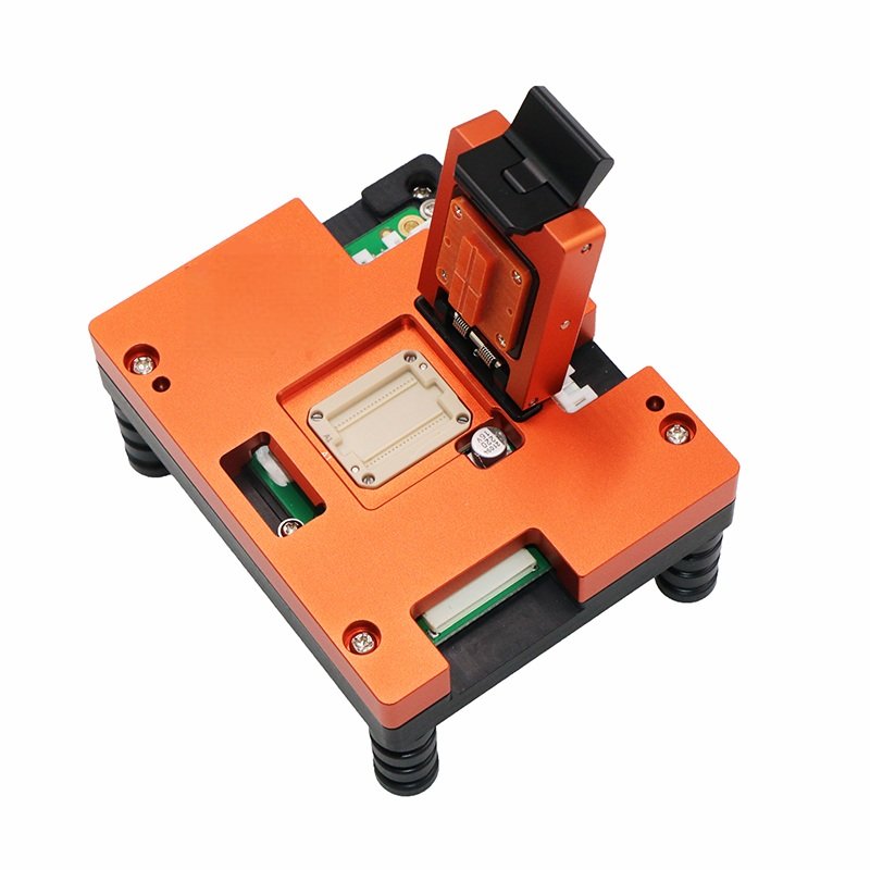
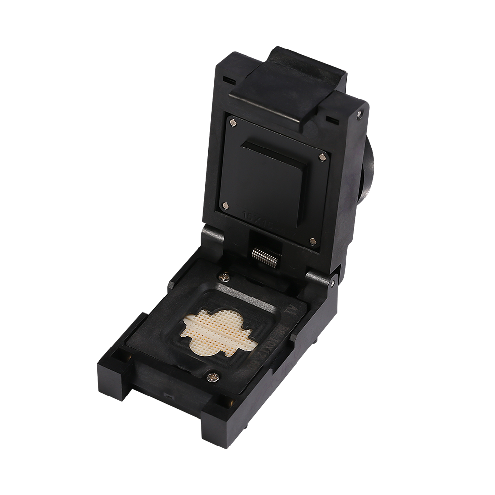
1) Semiconductor IC Test Fixture
Designed for consistent electrical/mechanical interfaces during functional and parametric testing. We focus on consistent location and controlled contact force to reduce re-test rates.
Design Priorities
- • Repeatable locating aligned to part datums
- • Serviceable wear parts (modular replacements)
- • Precision alignment to prevent skewing

2) Jigs & Fixtures for Encapsulations
Supporting processes where positioning during material application and curing is critical. We manage thermal stability and material flow to avoid residue traps.
- Thermal stability for curing cycles
- Relief features for overflow management
- Scratch-free protective contact points
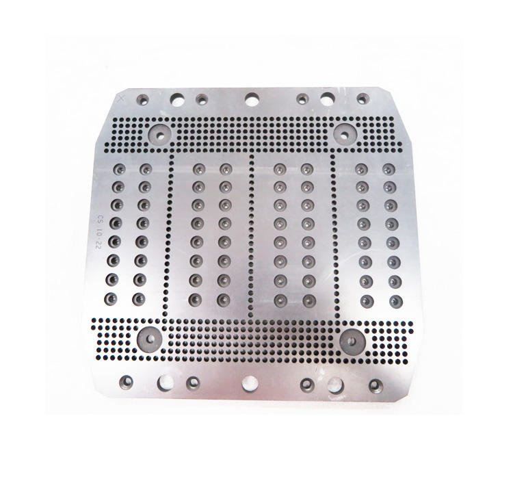
3) Semiconductor Vacuum Fixtures
Stable, low-distortion holding for thin, delicate substrates. Success is measured by flatness control and sealing stability rather than just raw suction force.
Zoned Vacuum Options
Control holding distribution and improve stability for warped parts.
Anti-Slip Surface Interaction
Designed to prevent micro-movement without marking the surface.

4) Semiconductor Chip Fixture
Position and protect chip-level components during micro-assembly and precision metrology. Micro-level repeatability is our core objective.
Micro-level Repeatability
Locating features designed for consistent seating and edge-safe handling.
Our Semiconductor Tooling Process
Input Review
Review drawings, cleanroom class, and ESD targets.
Locating Strategy
Determine datum references and support mapping.
Concept Design
Accessibility check and manual/robotic interface.
Validation
Functional checks and repeatability try-outs.
Capabilities Beyond Machining
We deliver fixtures that are usable and controllable—not just “built to drawing.”
Why Buyers Choose Us
-
Yield-Minded Engineering
ESD, particles, and deformation are designed-in risk factors.
-
Modular Tooling
Replaceable components ensure lower lifecycle costs.
-
Rapid Iteration
Change-friendly workflow to catch issues before ramp.
What We Need to Quote
- 2D/3D (STEP) Files
- Application Context
- ESD/Cleanroom Targets
- Sensitive Zones Notes
Send your current files—we’ll propose a safe concept first.
Semiconductor Tooling FAQ
What repeatability can you achieve?
How do you handle ESD requirements?
Stabilize Your Yield
Send your drawing and process points. We’ll reply with a DFM Review and a quote.